Cn

About Us

About Us

About Us
Company

Jade Bird Display

shanghai
Shanghai headquarters

Jade Bird Display (JBD), founded in 2015, is headquartered in Pudong, Shanghai, with a branch in Hefei, Anhui Province. Long dedicated to the development and production of MicroLED displays, it now boasts a series of independent technologies including IC design, MOCVD material growth, MicroLED hybrid integration, processing and manufacturing, packaging and testing, and software & hardware drive design. JBD has independently developed world-leading ultra-microdisplays, and injected strong momentum into technological advances across various fields including mixed reality, automobiles and semiconductors. Building on its core display technologies, JBD has skillfully combined integrated circuits and displays to deliver an array of hi-tech products including monochromatic/trichromatic displays, AM-µLED micro display development kits, AM-µLED displays, AM-µLED optical engines and optical modules, among others.

FAQs
Q Can you provide a brief introduction of JBD?
A

JBD is a manufacturer of MicroLED microdisplays. We operate on a Fab model and we manufacture our MicroLED microdisplays in our Fab based in Shanghai and we are expanding our production capacity by opening up a new fab in Hefei which will be operational at the end of 2022. In addition to MicroLED microdisplays we also have develop our light engines and projectors using our MicroLED displays for AR applications.

Q What are JBD's core competencies for manufacturing MicroLED microdisplays?
A

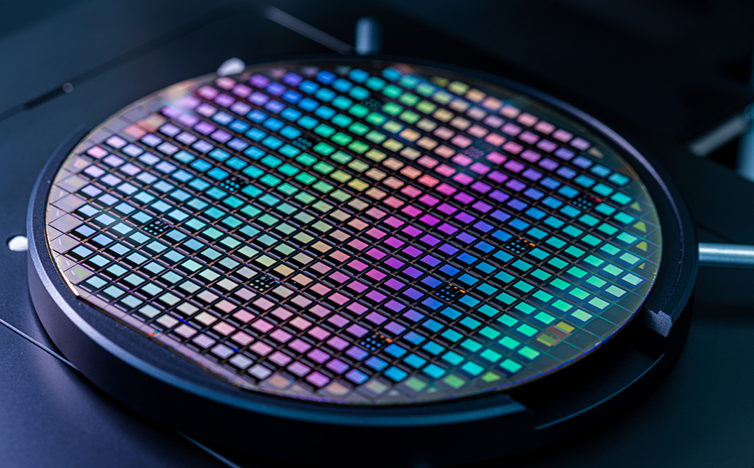
JBD uses a wafer level manufacturing process called monolithic hybrid integration, which involves wafer-level integration of group III-V and III-Nitride compound semiconductor materials on Si IC. Unlike pick-n-place and mass transfers techniques used by some MicroLED companies, JBD uses monolithic techniques, similar to CPU or DRAM manufacturing processes, to fabricate microdisplay chips/panels. Unlike most of the MicroLED displays with sizes larger than 1 inch (for watches, smartphones, TV etc), JBD is focusing on display panels less than 0.5 inch (12 mm ) in diagonal. Our MicroLED displays are developed using our patented wafer level manufacturing technology which includes the growth of LED light-emitting materials, the design of silicon-based CMOS backplane, chip processing, design & fabrication of MicroLens Array (MLA) and packaging and testing. This differentiates JBD from our peers as we are a MicroLED microdisplay manufacturer in comparison to establishments that classify themselves as MicroLED manufacturers solely focusing on the development of MicroLED emitters.

Q What products does JBD have?
A

JBD's MicroLED product portfolio includes 0.13" 480P R,G , B & UV MicroLED displays, 0.31" 720P R , G , B & UV MicroLED displays, and 0.22 " 1080P R, G & B MicroLED displays, of which 0.31" and 0.22" are mainly used to support development of custom display developments, especially for end products requiring large FOV (>50°).
The 0.13" series of MicroLED displays are in mass production. Small size and low power consumption are its core competency. JBD also launched a series of MicroLED projectors, including optical engine with waveguide, which can support rapid prototyping and quick turn around times for proof-of-concept builds.

Q Where are JBD MicroLED displays mainly used?
A

Due to its ultra-compact footprint, high brightness and low power consumption, JBD's MicroLED displays are widely used in AR near-eye display, micro projection (especially portable micro projection), sports optics, HUD for motorcycles, light field displays, 3D printing etc.

Q What is the approach to achieve full-color display of JBD?
A

A full-color monolithic panel is under development with native R, G & B sub-pixels. To address information based applications JBD currently offers a polychrome projector. The polychrome projector comprises of a x-cube prism, used to combine images from three individual monochrome panels attached to the faces of the X-cube prism. Another solution for a full-colour near-eye display is to couple our monochrome R, G & B projectors into waveguides with multiple input couplers to combine the individual R, G & B images from the three projectors.
The polychrome projectors are available to OEMs for development of end products, please contact us.

Q What is the power consumption of JBD MicroLED display?
A

The CMOS backplane of JBD adopts active matrix driving technology and internal compression algorithm, which effectively saves power consμmption. JBD has been focusing on developing the efficiency of MicroLED for many years, which is at the leading level in the industry. When only prompt information is displayed, the typical power consumption of MicroLED under the maximum brightness shall not exceed 100 mw.